

MOCVD Susceptor Factory: Precision Manufacturing for Semiconductor Epitaxy
2026-11-16
Ask any epitaxy engineer what keeps them up at night, and MOCVD susceptor performance will likely top the list. Poor thermal uniformity, particle generation, warping — they all trace back to manufacturing quality. Semicorex takes a different route: aerospace-grade precision for every susceptor that leaves the factory. Let’s unpack what that actually means.
Isotropic Graphite Selection for Thermal Stability at 1,100°C
When pushing graphite components to 1,100°C, the first filter isn't just purity or density—it's how evenly the material expands in every direction. Standard extruded graphite often hides directional stress that shows up as microcracking after repeated thermal cycles. For sustained exposure at this temperature, look for an isostatically pressed grade with a grain size under 10 µm and a coefficient of thermal expansion (CTE) spread of less than 0.3 × 10⁻⁶/K between axial and radial directions. That narrow delta is what keeps bolt threads, crucibles, and heating elements from loosening or binding after the first full ramp.
Thermal conductivity also plays a bigger role than many realize. A high-conductivity isotropic graphite—typically above 80 W/m·K at room temperature—pulls heat away from hot spots and reduces internal temperature gradients. At 1,100°C, that translates into fewer stress risers near sharp corners or thin walls. Pair that with a flexural strength that stays above 40 MPa after baking, and you get a material that survives rapid heat-up rates without the brittle failure common in cheaper anisotropic grades.
Finally, don't ignore the atmosphere. Even trace oxygen at 1,100°C will attack graphite, so if your furnace isn't running a tight vacuum or inert gas blanket, choose an oxidation-resistant grade with a proven inhibitor package, or limit continuous exposure times. Specifying a fine-grained, isostatically molded graphite with documented dimensional stability after thermal cycling is often the difference between a component that lasts hundreds of cycles and one that fails during commissioning.
CNC Pocket Machining with Sub-5 Micron Depth Uniformity
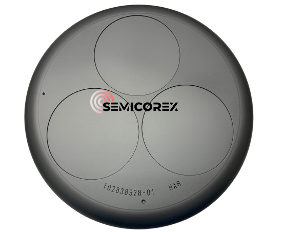
Achieving sub-5 micron depth uniformity across a CNC machined pocket demands a level of process control that goes well beyond standard milling practices. The pocket floor, typically generated by a flat end mill making overlapping passes, is highly sensitive to tool deflection, spindle thermal growth, and minute inconsistencies in workpiece fixturing. Even a few microns of variation can emerge from the natural sag of the tool between passes or from slight angular misalignment of the machine's axes. To hold depth variation under five microns, machinists often combine in-process probing with micro-step finishing passes, verifying the actual cut surface after roughing and semi-finishing before committing to a final skim cut of only a few microns.
One practical approach involves using a high-precision touch probe to map the pocket floor at multiple points, then compensating for measured errors through tool length offsets or by adjusting the Z-axis position on a point-by-point basis during a final pass. For shallow pockets, the use of a single, very light finish pass with a sharp, low-runout end mill helps minimize cutting forces and the associated tool deflection. Coolant temperature stability also plays a significant role, as thermal expansion of the spindle and workpiece can easily exceed several microns over the duration of a machining cycle. Some shops actively control coolant temperature or allow the machine to thermally stabilize before final depth cuts.
Material choice and toolpath strategy further influence the attainable uniformity. Softer, gummy materials may exhibit local elastic recovery that varies with grain direction, while harder materials can cause progressive tool wear that changes the effective depth of cut across the pocket. A common tactic is to use a climb milling strategy with a high helix angle and a small radial engagement, reducing radial forces that bow the tool. In production environments, periodic measurement of a reference pocket on a sacrificial part helps detect drift before it exceeds the five-micron window. Ultimately, sub-5 micron depth uniformity is not achieved by a single setting but by a tightly integrated loop of measurement, compensation, and controlled cutting parameters.
Silicon Carbide Coatings That Resist Ammonia Etching
Silicon carbide coatings have gained a reputation for standing up to some of the harshest chemical environments in modern manufacturing. When exposed to ammonia-based etch chemistries, these films do not readily degrade, thanks to their dense crystalline structure and the strength of the silicon-carbon bond. This makes them a practical choice for protecting reactor walls, susceptors, and other components that would otherwise suffer rapid material loss.
The resistance to ammonia etching comes from more than just chemical stability. High-quality SiC coatings are typically deposited with very low porosity, preventing ammonia and reactive byproducts from reaching the underlying substrate. Even at elevated temperatures, the surface remains passive, forming a thin oxide layer that further shields the bulk material. In side-by-side tests, silicon carbide consistently outperforms quartz, alumina, and many metals in ammonia-containing plasmas.
Typical application areas include etch chambers for compound semiconductors and LED fabrication, where ammonia and hydrogen mixtures are frequently used. Coatings are often applied by chemical vapor deposition to achieve uniform thickness and strong adhesion. By extending the lifetime of critical parts and reducing particle generation, silicon carbide coatings help maintain process stability and lower overall operating costs.
Thermal Cycling Protocols to Prevent Susceptor Warpage
Susceptor warpage often stems from uneven thermal expansion when heating and cooling rates exceed what the material can accommodate. A practical protocol starts with mapping the temperature distribution across the part using embedded thermocouples or an IR camera. The goal is to keep the edge-to-center differential below a set limit—typically 10–15°C for graphite susceptors—before moving to the next ramp step. Without this step, the outer rim heats or cools faster than the core, creating residual stress that accumulates over repeated cycles.
Instead of a single linear ramp, use a stepped profile with holds at intermediate temperatures. For a graphite susceptor with SiC coating, ramp at no more than 5°C/min up to 300°C, hold for 15–20 minutes to allow thermal equalization, then continue at 3°C/min to the process temperature. On the cooling side, avoid forced gas quenching; let the susceptor cool in the chamber at a controlled rate of 2–4°C/min until it drops below 150°C. This slower return to ambient prevents the sharp contraction that pulls the edges upward.
For susceptors already showing early signs of warpage, a dedicated stress-relief cycle can be applied once every 20–30 process runs. Heat the susceptor to about 80% of its maximum rated temperature, hold for two hours, and then cool at the same controlled rate without opening the chamber. This anneals micro-stresses before they turn into permanent deformation. Also rotate the susceptor periodically if the heater layout creates a fixed hot zone, as this balances the thermal history across the surface.
Custom Susceptor Designs for GaN-on-SiC and InP Epitaxy
Growth of GaN-on-SiC and InP heterostructures places extreme demands on temperature uniformity across the wafer. Standard susceptor pockets often create radial thermal gradients that lead to wafer bow, slip lines, or uneven ternary composition. Custom designs start with mapping the actual heat flux inside the reactor, not just the setpoint temperature.
One approach is to vary the local thermal mass of the susceptor by machining shallow recesses or adding inserts beneath the wafer. A slightly recessed pocket edge can reduce edge cooling, while a tailored backside contact pattern alters conductive coupling without trapping gas. High-purity SiC-coated graphite remains the usual choice, but its thickness and coating roughness are adjusted to match the emissivity profile of each wafer type.
Iterative prototyping with pyrometry and in-situ curvature sensors shows that even a 5°C reduction in edge-to-center delta improves InP photoluminescence uniformity and GaN buffer breakdown yield. The final susceptor often looks unconventional, with asymmetric mass distribution or venting channels, but it is tuned to a particular reactor geometry rather than copied from a generic design.
In-House Metrology for Surface Finish and Wafer Flatness
Keeping surface finish and wafer flatness measurements under one roof changes how quickly process deviations get caught. Instead of waiting on external labs, the fab compares roughness traces from a white-light interferometer against post-polish target ranges, often holding Ra below 0.5 nm on prime substrates. Flatness data is pulled from a capacitive wafer gauge, with total thickness variation and local site flatness reviewed alongside edge roll-off to catch subtle carrier or pad wear issues.
Daily calibration loops are tied to reference mirrors and quartz wafers, so drift shows up before it reaches product lots. The team tracks the same 25-point thickness map on every incoming wafer and flags any repeatable pattern shift, whether it comes from slurry distribution or a worn retaining ring. This makes the metrology data a working record rather than a pass-fail stamp.
When a lot falls outside the upper control limit, the in-house setup allows immediate cross-checks between optical profilometry and capacitance-based flatness tools. That overlap matters because some surface features look different depending on the measurement principle, and resolving those mismatches internally keeps corrective actions grounded in actual wafer geometry.
FAQ
We primarily use high-purity graphite substrates coated with silicon carbide (SiC). The graphite core provides excellent thermal conductivity and machinability, while the SiC layer adds chemical resistance and protects against reactive process gases.
Each susceptor undergoes CNC machining with tolerances within a few microns. We then verify critical dimensions using coordinate measuring machines and laser scanning, adjusting tool paths based on real-time feedback to maintain repeatability.
Yes, our SiC-coated graphite susceptors are rated for continuous operation up to 1600°C in reducing or inert atmospheres. The coating remains stable under thermal cycling, reducing particle generation and wafer contamination.
They are widely used in LED production, laser diodes, power electronics, and RF devices. Any process requiring uniform gallium nitride or aluminum gallium nitride epitaxy on sapphire, silicon, or silicon carbide wafers can benefit from our susceptor geometry control.
We optimize pocket depth, spacing, and thickness profiles to compensate for edge cooling effects. Finite element thermal modeling guides these adjustments, so a wafer sees less than ±2°C variation during growth, which directly improves wavelength and thickness uniformity.
Each batch undergoes visual inspection under bright light, ultrasonic scanning to detect coating delamination, and electrical resistivity checks on the SiC layer. We also run a simulated heating cycle to verify no outgassing or dimensional drift occurs.
Absolutely. Customers provide reactor drawings or wafer specifications, and we adapt pocket layouts, gas flow channels, and overall dimensions. Prototyping is fast, and we use rapid thermal testing to validate the custom geometry before mass production.
Conclusion
Inside a dedicated susceptor production line, the first decisions revolve around material behavior at temperature. Isotropic graphite is screened batch by batch for its ability to hold dimensions and thermal properties steady through repeated excursions to 1,100°C. Once a block passes incoming inspection, five-axis CNC pockets are milled with a depth tolerance tighter than five microns across the full face—an exacting target that prevents local hot spots during wafer heating. The machined surface then receives a dense silicon carbide coating formulated to endure ammonia-rich process gases without pitting or delamination, which is a common failure point in GaN MOCVD environments.
Beyond the core machining, each susceptor follows a staged thermal cycling schedule before it ever reaches a customer. These cycles mimic the ramp rates and soak times of real epitaxy runs, allowing the graphite and coating to settle together and revealing any latent tendency to warp. For GaN-on-SiC and InP platforms, pocket geometry, edge exclusion, and gas flow relief features are adjusted case by case, often starting from the customer's wafer map and reactor model. In-house metrology closes the loop, combining white-light interferometry for surface roughness with full-wafer flatness scans to confirm that the finished susceptor meets both local finish and global planarity requirements.
Contact Us
Contact Person: Svenja Wei
Email: [email protected]
Tel/WhatsApp: +8613567891907
Website: https://www.semicorex.com